Nanotechnology requires the ability to understand and precisely manipulate and control matter at the nanoscale in a useful way. Working at this small scale requires the ability to both “see” and manipulate nanomaterials in order to take advantage of their special properties.
How do scientists “see” what’s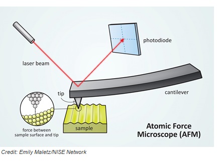 going on in the extremely small world of nanotechnology? The microscopes that are typically used in high schools are not able to image at this size scale. As early as the 1930s, scientists have been able to image at the nanoscale using instruments such as the scanning electron microscope, the transmission electron microscope, and the field ion microscope, but these techniques can require extensive sample preparation and are expensive. The invention of the scanning tunneling microscope (STM) and the atomic force microscope (AFM) in the 1980s is widely credited with opening up the field of nanotechnology. These microscopes can image a surface by scanning a tip over the surface and measuring the electron tunneling or interatomic forces, respectively. The STM can also be used to manipulate atoms on the surface, for example to create a quantum well There is now a broad suite of scanning probe microscopes that image an array of material properties including magnetic probe, electrostatic properties, etc.
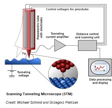
More information on the development of microscopic tools can be found on the “Nanotechnology Timeline” and at the following links:
- How the optical microscope became a nanoscope, The Nobel Prize in Chemistry 2014, The Royal Swedish Academy of Sciences
- Molecular Expressions—Science, Optics and You, Florida State University
Some Nanomaterials are named for their shapes and dimensions. Think of these simply as particles, tubes, wires, films, flakes, or shells that have one or more nanometer-sized dimensions. For example, carbon nanotubes have a diameter in the nanoscale, but can be several hundred nanometers long or even longer. Nanofilms or nanoplates have a thickness in the nanoscale, but their other two dimensions can be much larger.
Manufacturing at the nanoscale is known as nanomanufacturing. Nanomanufacturing involves scaled-up, reliable, and cost-effective manufacturing of nanoscale materials, structures, devices, and systems. It also includes research, development, and integration of top-down processes and increasingly complex bottom-up, or self-assembly, processes. Top-down fabrication reduces large pieces of material down to the nanoscale, 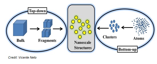 like someone carving a model airplane out of a block of wood. The bottom-up approach to nanomanufacturing creates products by building them up from atomic- and molecular-scale components. Bottom-up approaches also include certain molecular-scale components that spontaneously “self-assemble” into ordered structures.
Within the top-down and bottom-up categories of nanomanufacturing, there are a growing number of new processes that enable nanomanufacturing. Among these are the following:
- Chemical vapor deposition is a process in which chemicals react to produce very pure, high-performance films.
- Molecular beam epitaxy is one method for depositing highly controlled thin films.
- Atomic layer epitaxy is a process for depositing one-atom-thick layers on a surface.
- Dip pen lithography is a process in which the tip of an atomic force microscope is “dipped” into a chemical fluid and then used to “write” on a surface, like an old-fashioned ink pen onto paper.
- Nanoimprint lithography is a process for creating nanoscale features by “stamping” or “printing” them onto a surface.
- Roll-to-roll processing is a high-volume process to produce nanoscale devices on a roll of ultrathin plastic or metal.
- Self-assembly describes the process in which a group of components come together to form an ordered structure without outside direction.

