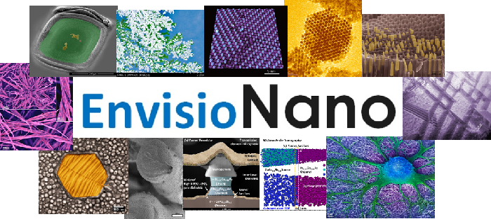
Iron HoneycombVikas Nandwana
Advisor: Vinayak Dravid
Department of Materials Science and Engineering
Northwestern University
 Caption: Hexagonal close-packed assembly of iron oxide nanoparticles
|
***************************************************
Description: The particles shown here are made of iron oxide, or rust – just like on a car. But these nanoparticles are tiny, 100,000 times thinner than a sheet of paper. At such a small size, they demonstrate some unique properties that can be used to detect and treat diseases like cancer by just applying external magnetic field without any side effects. Due to the same size and shape, the magnetic nanoparticles self-assemble (or come together) into a closely-packed honeycomb pattern. Iron oxide nanoparticles like these are already used to help people suffering from iron deficiency (anemia). Researchers study how these magnetic nanoparticles interact with each other and tissues in the body, which can open new avenues for nontoxic, targeted tests and treatments for cancer, Alzheimer’s and cardiovascular disease. Laboratory website: http://vpd.ms.northwestern.edu/ Technique: Transmission Electron Microscopy Funding Source: NTU-NU Institute for NanoMedicine located at the International Institute for Nanotechnology, Northwestern University, USA and the Nanyang Technological University, Singapore. |
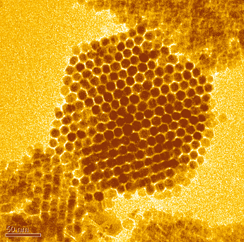
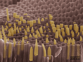
Tunnel Field-Effect-TransistorRahul Pandey
Advisor: Dr. Suman Datta, EE, Pennsylvania State University and University of Notre Dame Department of Electrical Engineering
Pennsylvania State University
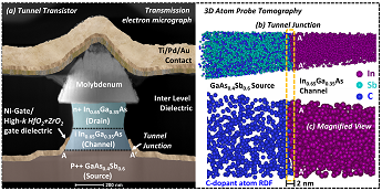 Caption: (a) Cross-section micrograph of Tunnel Field-Effect-Transistor (TFET). TFETs are high impact next generation transistors which can provide high performance with extreme energy efficiency compared to conventional silicon-transistors. This high performance stems from quantum mechanical tunneling of electrons across the tunnel junction interface detailed in (b) and (c). TFET fabrication and Transmission Electron Micrograph by Rahul Pandey. Atom Probe characterization of TFET tunnel junction done in collaboration with Markus Kuhn at Intel Corporation (Metrology Group, Hillsboro, OR).
|
Want to vote for this image?
*************************************************** Description: As we venture into the era of Internet of Things with more intelligent and connected electronic devices, there is an increasing need for more energy efficient data processing. Conventional Silicon-MOS Field-Effect-Transistors (MOSFETs) cannot meet these demands. We are developing a Tunnel Field-Effect-Transistor (TFET) based on III-V arsenide-antimonide hetero-junctions to provide high performance at extremely low power consumption. In a TFET, the electrons undergo quantum mechanical tunneling from the source to the channel region which filters out the high-energy carriers resulting in very steep switching and energy savings. Using III-V arsenide-antimonide hetero-junctions in designing TFETs ensures high performance through high on-current even at extremely low voltages (<0.5 V). Critical to TFET performance when they are made from combinations of III-V materials is the need for abrupt and uniform interfaces among the dissimilar materials. Variability at these interfaces, or heterojunctions, dramatically impacts device performance. It is hence of significant importance to characterize hetero-junction TFETs with precision in nanometer-scale devices which have been presented in the figures. Laboratory website: http://www.ndcl.ee.psu.edu/
Technique: Cross-section micrograph of fabricated III-V compound semiconductor based TFET (Fig. a) is obtained through Transmission Electron Microscopy (TEM). The team at Penn State collaborated with researchers from Intel Corporation to use Atom Probe Tomography and Time-of-flight Spectroscopy to characterize critical tunnel junction interface in TFET (Fig. b and c). Funding Source: This work was supported by the National Science Foundation ASSIST Nanosystems ERC under Award Number EEC-1160483.
|
Nano SheepOnur Ergen
Advisor: Alex Zettl
Department of Physics
University of California, Berkeley
 Caption: Smiling in Nanospace (Nano=sheep) Caption: Smiling in Nanospace (Nano=sheep) |
***************************************************
Description: ZnO nanowires are grown on Cu wire without any catalysis. These nanowire assemblies serve as optically active multi-purpose templates. Various solar and piezoelectric energy harvesting devices can be prepared using this architecture. Moreover, it is an essential building block for variety of novel electrochemical and photochemical devices. Laboratory website: http://research.physics.berkeley.edu/zettl/ Technique: Scanning Electron Microscopy Funding Source: This research was supported in part by the Director, Office of Science, Office of Basic Energy Sciences, Materials Sciences and Engineering Division of the U.S. Department of Energy under Contract No. DE-AC02-05CH11231, which provided for SEM imaging under an LDRD award, and, within the sp2-bonded materials program (KC2207), for the design of the experiment and material characterization; the National Science Foundation under Grant 1542741, which provided for photovoltaic response characterization; and by the Office of Naval Research (MURI) under Grant N00014-12-1-1008, which provided for nanowire growth.
|
Graphene Shows its StripesBen Davis
Ryan Hines
Advisor: Matt Maschmann
Department of Mechanical and Aerospace Engineering
University of Missouri
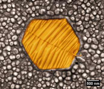 Caption: The SEM micrograph shows an isolated and wrinkled hexagonal graphene grain supported on copper. Graphene is a 2-D material with mechanical, electrical, and thermal properties that exceed conventional engineering materials. Caption: The SEM micrograph shows an isolated and wrinkled hexagonal graphene grain supported on copper. Graphene is a 2-D material with mechanical, electrical, and thermal properties that exceed conventional engineering materials. |
Want to vote for this image?
*************************************************** Description: This grain of graphene was synthesized using chemical vapor deposition on a copper foil substrate. The hexagonal shape of the graphene grain is indicative of the graphene hexagonal crystal lattice structure, while the striped pattern arises due to adhesion and wrinkling with the underlying substrate. To fully capitalize on the potentially transformative physical properties of graphene, we are examining methodologies to locally machine carbon nanomaterials such as graphene with the spatial resolution consistent with that of scanning electron microscopes (~2 nm). This image was taken prior to machining; however, a small rhombus-shaped test hole may be seen near the bottom right face of the graphene crystal. Through innovative nanomanufacturing, we hope to design highly efficient nanoscale transistors and devices with areal densities greater than current integrated circuits. Laboratory website: http://engineers.missouri.edu/maschmannm/ Technique: Transmission Electron Microscopy
Funding Source: This work is funded by the University of Missouri Alumni Association Richard Wallace Faculty Incentive Grant.
|
Nanoscale Stadium Made from a Carbon Nanotube ForestBen Davis
Advisor: Matt Maschmann
Department of Mechanical and Aerospace Engineering
University of Missouri
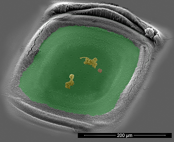 Caption: The SEM micrograph shows large collection of vertically aligned carbon nanotubes, along with amorphous carbon in the shape of tigers and a ball. Carbon nanotubes are 1-D material with mechanical, electrical, and thermal properties that exceed conventional engineering materials. Caption: The SEM micrograph shows large collection of vertically aligned carbon nanotubes, along with amorphous carbon in the shape of tigers and a ball. Carbon nanotubes are 1-D material with mechanical, electrical, and thermal properties that exceed conventional engineering materials. |
Want to vote for this image?
*************************************************** Description: This “forest” of vertically aligned carbon nanotubes was synthesized using chemical vapor deposition (CVD) on a self-heating substrate. The radial pattern of nanotubes with different heights is indicative of a temperature gradient on the substrate and, consequently, a gradient of growth rates. To fully capitalize on the potentially transformative physical properties of carbon nanotubes, we are examining the growth mechanisms of nanotubes in CVD, as well as a method to locally machine carbon nanomaterials with the spatial resolution of ~2 nm. This image was taken prior to machining. Through innovative nanomanufacturing, we hope to design highly efficient nanoscale transistors and devices with areal densities greater than current integrated circuits. Laboratory website: http://engineers.missouri.edu/maschmannm/
Technique: Scanning Electron Microscope. False color using Adobe Photoshop. Funding Source: This work is funded by the University of Missouri Alumni Association Richard Wallace Faculty Incentive Grant.
|
Stacks of DefectsEmily Hoffman
Advisor: Laurence Marks
Materials Science and Engineering
Northwestern University
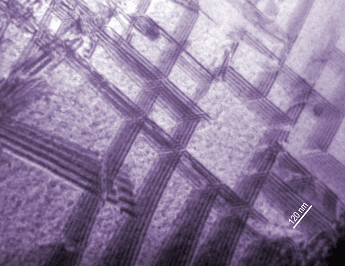 Caption: This is a transmission electron microscope image of a metal alloy of cobalt, chromium, and molybdenum. The sample is about 100 nm thick, letting electron pass through the sample to make the image. The dark lines are defects in the metal crystal. We are seeing preferentially arranged stacks of defects. Caption: This is a transmission electron microscope image of a metal alloy of cobalt, chromium, and molybdenum. The sample is about 100 nm thick, letting electron pass through the sample to make the image. The dark lines are defects in the metal crystal. We are seeing preferentially arranged stacks of defects. |
Want to vote for this image?
*************************************************** Description: I work on the metal alloy used for hip replacements. Improving biomaterials can have a major impact on the aging population – we’ll need over 500,000 hip implants per year by 2030. I am trying to understand the metal alloy at the nanoscale. The goal is to reduce corrosion and wear that occurs at the joint in an implanted hip. By using transmission electron microscopy, I can look at the metal on the atomic level of the crystal. We can see the variations in chemical composition and crystal structure. These defects can be the initiation point for the metal to break down. Through designing better biomaterials, we can have safe and durable implants. Laboratory website: Northwestern NUANCE Center, Electron Probe Instrumentation Center (EPIC) http://www.nuance.northwestern.edu/index.html
Technique: Transmission electron microscopy, JEOL 2100 in TEM mode, bright field imaging Funding Source: National Science Foundation grant number CMMI-1030703
|
Nano HerringboneXiaolong Liu
Advisor: Mark Hersam
Applied Physics Program
Northwestern University
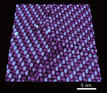 Caption: The image shows molecules of perylenetetracarboxylic dianhydride self-assembling on the surface of a silver crystal, forming well-ordered herringbone-like patterns with periodic height variations. Three molecular domains touch each other and form three grain boundaries. Caption: The image shows molecules of perylenetetracarboxylic dianhydride self-assembling on the surface of a silver crystal, forming well-ordered herringbone-like patterns with periodic height variations. Three molecular domains touch each other and form three grain boundaries. |
Want to vote for this image?
*************************************************** Description: My current research focuses on exploring functionalized two dimensional (2D) nanomaterials at the molecular and atomic scales using scanning tunneling microscopy and spectroscopy (STM/STS). Junctions formed by self-assembled organic monolayers and 2D nanomaterials (e.g., graphene) are promising candidates for next generation electronics, especially for flexible devices. The examination of fundamental properties such as grain boundaries, defects and molecule conformations via STM/STS would greatly facilitate rational choice of molecules, as well as revealing interface properties that are essential before such junctions can be employed in real world applications. This image gives an example of a monolayer of self-assembled perylenetetracarboxylic dianhydride molecules, highlighting the three grain boundaries formed from three merging grains. In addition to the herringbone structures of the self-assembled molecules, periodic height modulations are observed for every other row. The grain boundaries might play an important role in affecting the electronic and seeding properties when used in electronics. Laboratory website: http://www.hersam-group.northwestern.edu/
Technique: Scanning Tunneling Microscopy Funding Source: U.S. Department of Energy SISGR program (DOE DE-FG02-09ER16109)
|
Gold NanorodsTaegon Oh
Advisor: Chad Mirkin
Northwestern University
 Caption: This electron micrograph shows gold nanorods which were synthesized and embedded in the nanopores of anodic aluminum oxide membrane. The nanorods were elongated and eventually fractured with conical shapes during the cracking of the nanoporous template. The image was colored to distinguish the gold nanorods (orange) from the template (red). Caption: This electron micrograph shows gold nanorods which were synthesized and embedded in the nanopores of anodic aluminum oxide membrane. The nanorods were elongated and eventually fractured with conical shapes during the cracking of the nanoporous template. The image was colored to distinguish the gold nanorods (orange) from the template (red). |
Want to vote for this image?
*************************************************** Description: Our current research is on the development of synthetic techniques and chemical modifications of 1-D nanostructures of template synthesis, and this image was taken during the characterization of an intermediate step. This parallel synthesis grows metallic nanowires embedded in the nanoporous template. After synthesis, the cracking of the membrane caused the collective fractures of gold nanorods. The conical shapes of the rods results from highly ductile fractures during the fracture and these resemble the uniaxial tensile testing of ductile materials. This observation suggests future experiments to characterize collective mechanical properties of the nanorod-template composites. The results of tensile testing are expected to vary depending on the dimensions and compositions of the nanorods. Laboratory website: http://mirkin-group.northwestern.edu/
Technique: Gold nanorod growth was performed by electrochemical template synthesis along nanoporous anodic aluminum oxide membrane. The sample was sputter-coated by 10 nm Au/Pd and the image was taken by Hitachi SEM SU8030. Funding Source: Office of Naval Research, Grant Number: N00014-11-1-0729
|
Neural Cell on NanofibersZaida Alvarez Pinto
Mark McClendon
Advisor: Samuel Stupp
Simpson Querrey Institute for BioNanotechnology
Northwestern University
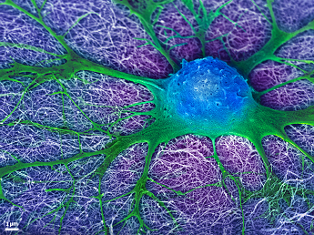 Caption: False color image of an embryonic neural cell (blue/green) derived from the mouse spinal cord and cultured on a synthetic nanofiber gel (purple). The prolongations of the cell (green) are extending throughout the nanofibers to re-establish a neural network with other cells. These nanofibers (~10nm in diameter) were specifically designed to encourage neural outgrowth by mimicking the environment of spinal cord tissue. Caption: False color image of an embryonic neural cell (blue/green) derived from the mouse spinal cord and cultured on a synthetic nanofiber gel (purple). The prolongations of the cell (green) are extending throughout the nanofibers to re-establish a neural network with other cells. These nanofibers (~10nm in diameter) were specifically designed to encourage neural outgrowth by mimicking the environment of spinal cord tissue. |
Want to vote for this image?
*************************************************** Description: Spinal cord injuries often lead to lifelong disabilities and the key to functional recovery is reconnecting the neuronal pathways that were damaged. One solution is to induce neural stem cells in the spinal cord to regenerate the cellular extensions while discouraging scar tissue formation that would otherwise block the reconnections from occurring. Shown in this image is a mouse neural cell growing on a synthetic nanofiber gel that has been designed to mimic the native environment of the spinal cord tissue. A local injection of these nanofibers following spinal cord injuries in mice was able to reduce glial scar formation and restore hind leg function with only one treatment.
More Info:
J. Neurosci., 28(14), (2008) 3814-3823
Journal of Neuroscience Research 88(14), (2010) 3161-3170
Biomaterials 43(20), (2013) 4749-4757
Biomaterials 35(1), (2014) 185-195
Biomaterials 35(31), (2014) 8780-8790
Laboratory website: http://stupp.northwestern.edu/group/index.html
Technique: Scanning Electron Microscopy, false color added with Photoshop. Funding Source:
National Institute of Health (NIH), Institute: National Institute of Biomedical Imaging and Bioengineering (NIBIB), Project #5R01EB003806-10 and Beatriu de Pinós Fellowship (AGAUR) |
Twisted NanofibersRonit Freeman
Mark McClendon
Advisor: Samuel Stupp
Simpson Querrey Institute for BioNanotechnology
Northwestern University
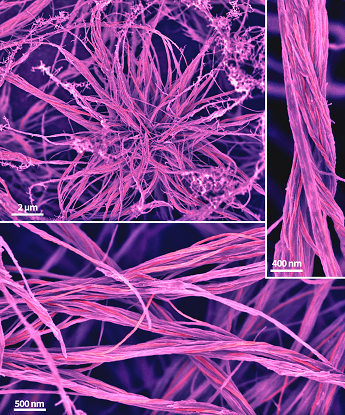 Caption: False color image of peptide nanofibers that have bundled and twisted together. Upper right panel shows that the individual nanofibers (~10nm diameter) start bundling in small groups of two or three nanofibers then these bundles begin twisting with neighboring bundles creating large braided structures similar to the organization of fibers in common rope. Caption: False color image of peptide nanofibers that have bundled and twisted together. Upper right panel shows that the individual nanofibers (~10nm diameter) start bundling in small groups of two or three nanofibers then these bundles begin twisting with neighboring bundles creating large braided structures similar to the organization of fibers in common rope. |
Want to vote for this image?
*************************************************** Description: Growing artificial organs and tissues is one challenge that nanotechnology strives to accomplish. The nanofibers shown here are made from biocompatible amino acids linked together (a.k.a. peptides). These nanofibers make excellent gels that can be used to grow cells and regenerate living tissue. The challenge is that every type of cell prefers a different gel stiffness. But these new nanofiber gels allow us to precisely tune the gel stiffness by controlling the amount of twisting in the nanofiber bundles. The twisted bundling behavior is a result of the attractive forces between the individual nanofibers. By introducing different soluble molecules to the gels we can switch on and off this twisting behavior thereby changing the gel stiffness for whatever specific cells are being cultured. Having this dynamic material on which to grow cells allows us to make very complicated scaffolds required for growing artificial tissues.
More Info:
Advanced Materials 26(11), (2014) 1642-1659.
Biomaterials 43(20), (2013) 4749-4757.
Biomaterials 33(23), (2012) 5713-5722.
Laboratory website: http://stupp.northwestern.edu/group/index.html
Technique: Scanning Electron Microscopy, false color added with Photoshop. Funding Source: National Institute of Health (NIH), Institute: National Heart, Lung, and Blood Institute (NHLBI), Project # 1R01HL116577-01A1, Program Officer: Danthi, Narasimhan
|
First SnowMichael Cai Wang (PhD candidate, sample preparation and characterization)
Department of Mechanical Science and Engineering
Siddhesh Dhanawade (BS candidate, sample preparation)
Department of Mechanical Science and Engineering
Grace Yao Hou (MS candidate, image manipulation)
Department of Statistics
Advisor: Prof. SungWoo Nam
Department of Mechanical Science and Engineering
University of Illinois at Urbana-Champaign
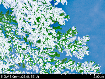 Caption: Electrochemical dendritic growth of copper and copper oxide on a monolayer graphene substrate appears as lightly snow-dusted juniper on a clear and brisk winter day. Caption: Electrochemical dendritic growth of copper and copper oxide on a monolayer graphene substrate appears as lightly snow-dusted juniper on a clear and brisk winter day. |
Want to vote for this image?
*************************************************** Description: The development of scalable, controllable, and rapid manufacturing techniques for laterally aligned metallic, semiconducting, and piezoelectric nanowires has great implications for flexible/wearable electronics, sensors, and energy harvesting devices. Here, we intended to achieve templated electrochemical synthesis of laterally (as opposed to the typical vertically) aligned copper nanowire arrays on a conductive monolayer graphene electrode. Mother Nature (and/or our lack of experimental finesse) decided instead that dendritic growth was more favorable and thus yielded a beautiful fractal-like pattern with some dispersed vertical particulate growth - not unlike a coniferous tree with a light sprinkling of snow on a beautiful, brisk, and clear winter day. In spite of the eye candy, we intend to refine our technique to achieve our original goal. Such developments will enable next generation of nano-materials and technologies that will help us preserve all that Mother Nature has given us: lush evergreens and chilly winters included. Laboratory website: http://nam.mechse.illinois.edu/
Technique: Image was acquired with a scanning electron microscope (Hitachi S4800) and false-colored in Photoshop. Funding Source: Air Force Office of Scientific Research/Asian Office of Aerospace Research Development (AFOSR/AOARD)
Program Manager: Mario Serna Grant Number: Nano Bio Info Technology (NBIT) Phase III Program AOARD-13-4125
|

