Nanotechnology is more than just mixing nanoscale materials together; it requires the ability to understand and to precisely manipulate and control those materials in a useful way.
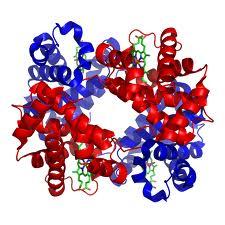 |
Computer simulation of hemoglobin, a naturally occuring nanoscale protein that |
Nanotechnology involves a new and broad science where diverse fields such as physics, chemistry, biology, materials science, and engineering converge at the nanoscale.
It is also important to understand that nanoscale materials are found in nature. For instance, hemoglobin, the oxygen-transporting protein found in red blood cells, is 5.5 nanometers in diameter. Naturally occurring nanomaterials exist all around us, such as in smoke from fire, volcanic ash, and sea spray. Some nanomaterials are a byproduct of human activity, such as bus and automobile exhaust and welding fumes.
You may recall from the Size of the Nanoscale page that the nanoscale is about 1 to 100 nanometers. Working at the nanoscale requires an understanding of the various types and dimensions of nanoscale materials. Different types of nanomaterials are named for their individual shapes and dimensions. Think of these simply as particles, tubes, wires, films, flakes, or shells that have one or more nanometer-sized dimension. For example, carbon nanotubes have a diameter in the nanoscale, but can be several hundred nanometers long or even longer. Nanofilms or nanoplates have a thickness in the nanoscale, but their other two dimensions can be much larger.
The key is to be able to both see and manipulate nanomaterials in order to take advantage of their special properties. As mentioned earlier, the invention of special microscopes gave scientists the ability to work at the nanoscale. The first of these new discoveries was the scanning tunneling microscope. While it’s mainly designed to measure objects, it can also move tiny objects such as carbon nanotubes.
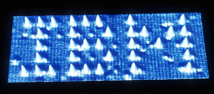 |
| IBM logo written with 35 xenon atoms on a copper substrate. (Image courtesy: IBM) |
The earliest example of this type of process was accomplished by IBM on November 11, 1989, when researcher Don Eigler and colleagues spelled the company logo in atoms. He and his team were able to literally move 35 xenon atoms on a background of copper atoms to spell out IBM.
More recently a team of Stanford University researchers led by Hari Manoharan were able to encode 35 bits of information per electron and write letters so small they are composed of subatomic bits of matter only 0.3 nanometers wide, or roughly one third of a billionth of a meter. In other words, they beat the record set by IBM, writing Stanford’s initials in letters smaller than atoms. These exercises demonstrated the precision with which it is possible to manipulate matter.
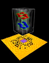 |
Artist's rendering of "SU" written in letters smaller than individual atoms. (Image courtesy: Stanford University)
|
Today, research scientists in universities and companies around the world are manufacturing nanomaterials to make new products and applications, from medical devices and drugs that may treat disease, to strong and lightweight materials that reduce fuel costs for cars and planes. For more information about these discoveries and inventions, see Benefits and Applications here on the Nano.gov website.

