The area of consumer electronics has already seen a profound impact from nanotechnology. Smaller and faster devices that are enabled by nanoscale features are made possible by advances in materials and processing technologies. Super-hydrophobic coatings make phones water resistant. Carbon nanotube-based electronics that are resistant to radiation have been flown on space missions. Quantum dots are being used in flat screen televisions. Yet, the most exciting advances in nanoelectronics are still under development! Nanotechnology will enable entirely new ways to store and manipulate information, and flexible electronics will be commonplace.
Fostering Cooperation to Advance Semiconductor Science and Technology
Continuing to shrink the dimensions of electronic devices is necessary to further increase processor speed, reduce device switching energy, increase system functionality, and reduce manufacturing cost per bit. However, as the dimensions of critical elements of devices approach atomic size, quantum tunneling and other quantum effects degrade and ultimately prohibit the operations of conventional semiconductor devices, and new conceptual solutions are necessary. In recognition of these limitations, the National Science Foundation (NSF) and the Semiconductor Research Corporation (SRC) have a long-standing Memorandum of Understanding to foster cooperation in research and education projects that can advance knowledge in the field of semiconductor science and technology and enhance the field’s use for the benefit of the industry, the Nation, and society. For example, in 2011, the NSF and the SRC’s Nanoelectronics Research Initiative (NRI) cooperated on the solicitation Nanoelectronics for 2020 and Beyond (NEB). The goal of NEB was to explore innovative research concepts in nanoelectronics. This research involved various avenues of study from novel materials, chemistry, and logic devices; to circuit designs, systems architectures, and algorithms; to new paradigms for computation, sensing, and processing of information. NSF and NRI jointly supported 12 four-year grants to interdisciplinary teams of investigators totaling $20 million.
Allowing Moore’s Law to Continue for Many Years to Come
| Nantero, one of Electronic Engineering Times’ 10 top startups to watch in 2013, has developed a carbon nanotube-based memory, NRAM. Funded in part by Air Force Small Business Innovation Research and Small Business Technology Transfer awards, Nantero’s NRAM switches in picoseconds, is permanently nonvolatile, consumes very little energy, and is scalable down to just a few nanometers in size. This technology enables true instant-on computers, faster servers, and data centers that consume much less power. For example, mobile devices could operate faster with longer battery life. In addition, the same carbon nanotube material and manufacturing processes used for NRAM can be used for next-generation transistors and interconnects, allowing Moore’s Law to continue for many years to come. |
|
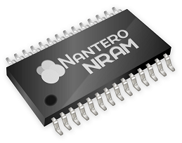 Nantero's next-generation memory NRAM Photo courtesy of Nantero, Inc.
Stretching, Folding, Twisting, and Not Damaging Electronics
Semiconductor nanomembranes (NMs) are single-crystal structures with thicknesses of less than a few hundred nanometers and with minimum lateral dimensions at least two orders of magnitude larger than the thickness. Silicon nanomembranes (SiNM) have many properties that are different from those of bulk silicon. They are flexible, conformal, transparent, strainable, transferable, bondable, stackable, and patternable. Advanced demonstration devices using NMs have been reported, perhaps most significantly in the area of flexible and stretchable electronics. NMs of silicon or germanium mounted on plastic or rubber substrates allow bending, stretching, folding, twisting, and other demanding modes of deformation without inducing damage or fatigue in the materials. Through Department of Defense Multidisciplinary Research Program of the University Research Initiative investments, the U.S. Government has significantly boosted activities in this frontier of materials nanotechnology. This activity is supporting leading researchers such as Max Lagally and Jack Ma (UWisconsin), Ray Chen (UT Austin), Hank Smith (MIT), and John Rogers (UIUC).
Efficient Electronic Assemblies without Using Hazardous Materials
Since the advent of current electronics, lead has been the primary solder material due to its low melting temperature. However, because of a worldwide effort to phase out hazardous materials in electronics, there is now an urgent need for lead-free solder. The common lead-free replacement, a combination of tin, silver, and copper, has multiple issues. It requires high processing temperatures, which drive costs up, the high tin content can lead to tin whiskers that can cause short circuits, and fractures are common in challenging environments. As a result, Defense-wide Manufacturing Science & Technology initiated a program in the area of "Solder Free Electronics." The idea was to develop a material and/or accompanying process to fabricate electronic systems that would obviate the need for commercial lead-free solders and eliminate their accompanying problems. Nanoparticle metals have an inherently reduced melting and fusing temperature when compared with bulk materials. By employing this effect, Dr. Alfred Zinn of Lockheed Martin Advanced Technology Center was able to develop a nanoparticle copper suspension, CuantumFuse™, which can be used to replace solder bonding in a standard electronics assembly process. Copper was chosen because it is already used throughout the electronics industry, is cheap (1/4th the cost of tin; 1/100th the cost of silver, and 1/10,000th the cost of gold), abundant, and has ten times the electrical and thermal conductivity of commercial tin-based solder, which can lead to more efficient electronic assemblies.

